Attenuated Total Reflectance (ATR)
$99 Base price View My Quote RequestTransmission Electron Microscopy (TEM)
Transmission electron microscopy (TEM) is the highest-resolution imaging technique available today. It is used to visualize sample features with atomic-level spatial resolution limits in order to characterize morphology of complex nanostructures.
“These are incredible images. Thanks for the preview.
It is so satisfying to get definitive answers to our questions!”
– Brad Aitchison, Sr. Process Engineer, Redlen Technologies
Strengths
- Highest possible spatial resolution: limit is atomic-scale
- Bright Field and Dark Field imaging
- Distinct imaging modes allow isolation of certain types of contrast information
- Compatible with chemical (EDS) analysis and electrochemical analysis (EELS) techniques
- Tomography and 3D reconstruction
Limitations
- Requires extensive sample prep (normally performed with a FIB-SEM)
- Specimens can be damaged if low dose techniques are not employed
- Minimal topographical sensitivity
- Typically only able to image a very small portion of the sample
Technical Specifications:
Learn More:
Example Outputs
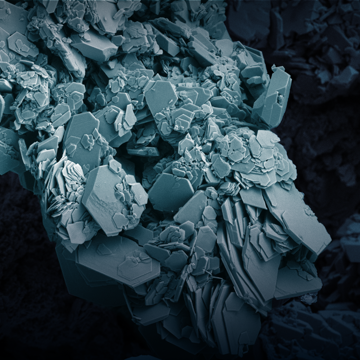
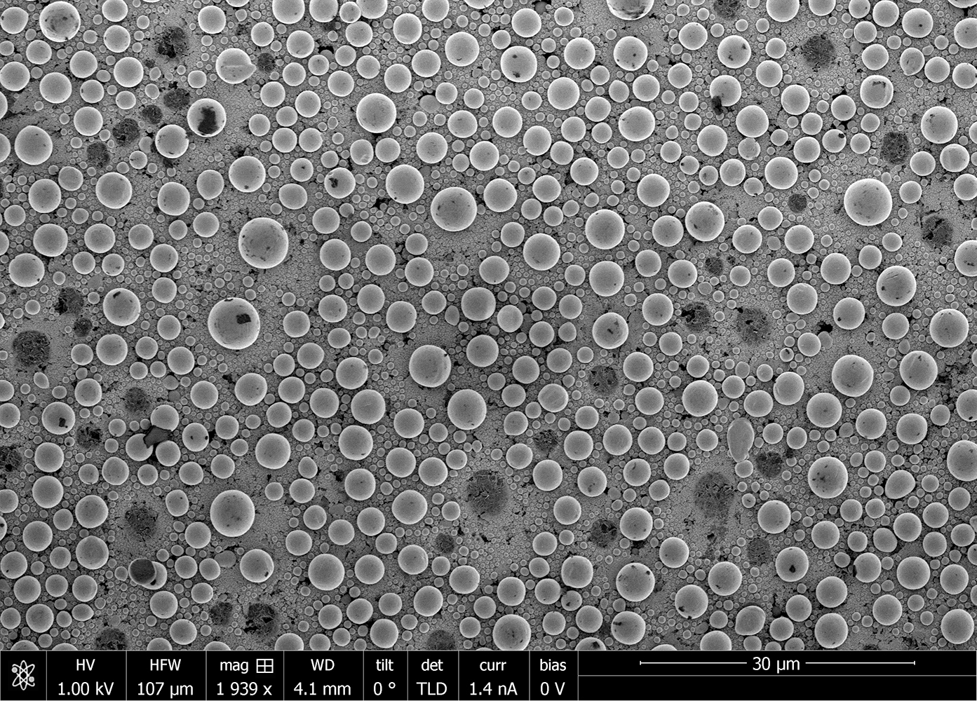
Ultra high resolution brightfield TEM image captured with the 4k Gatan OneView camera.
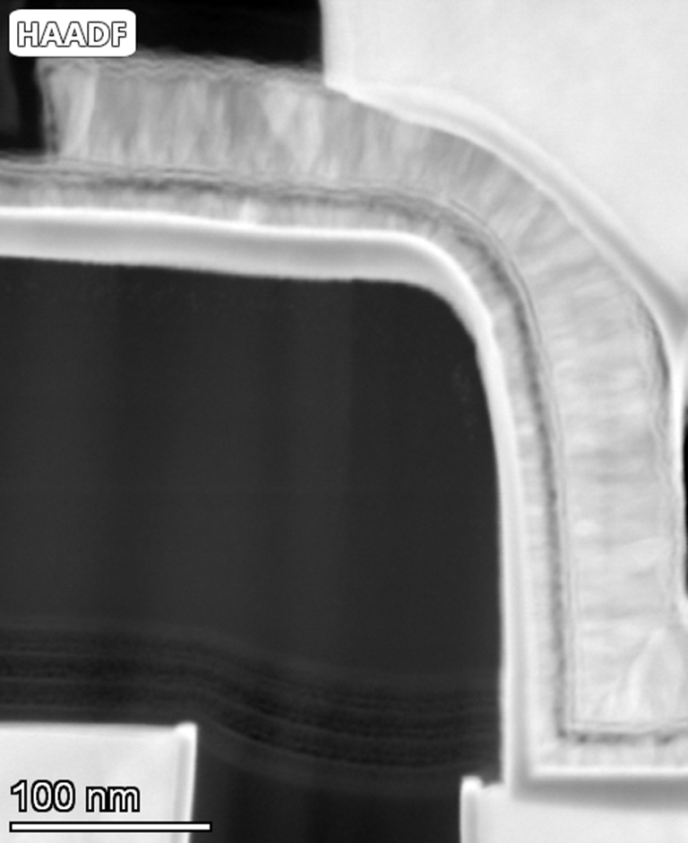
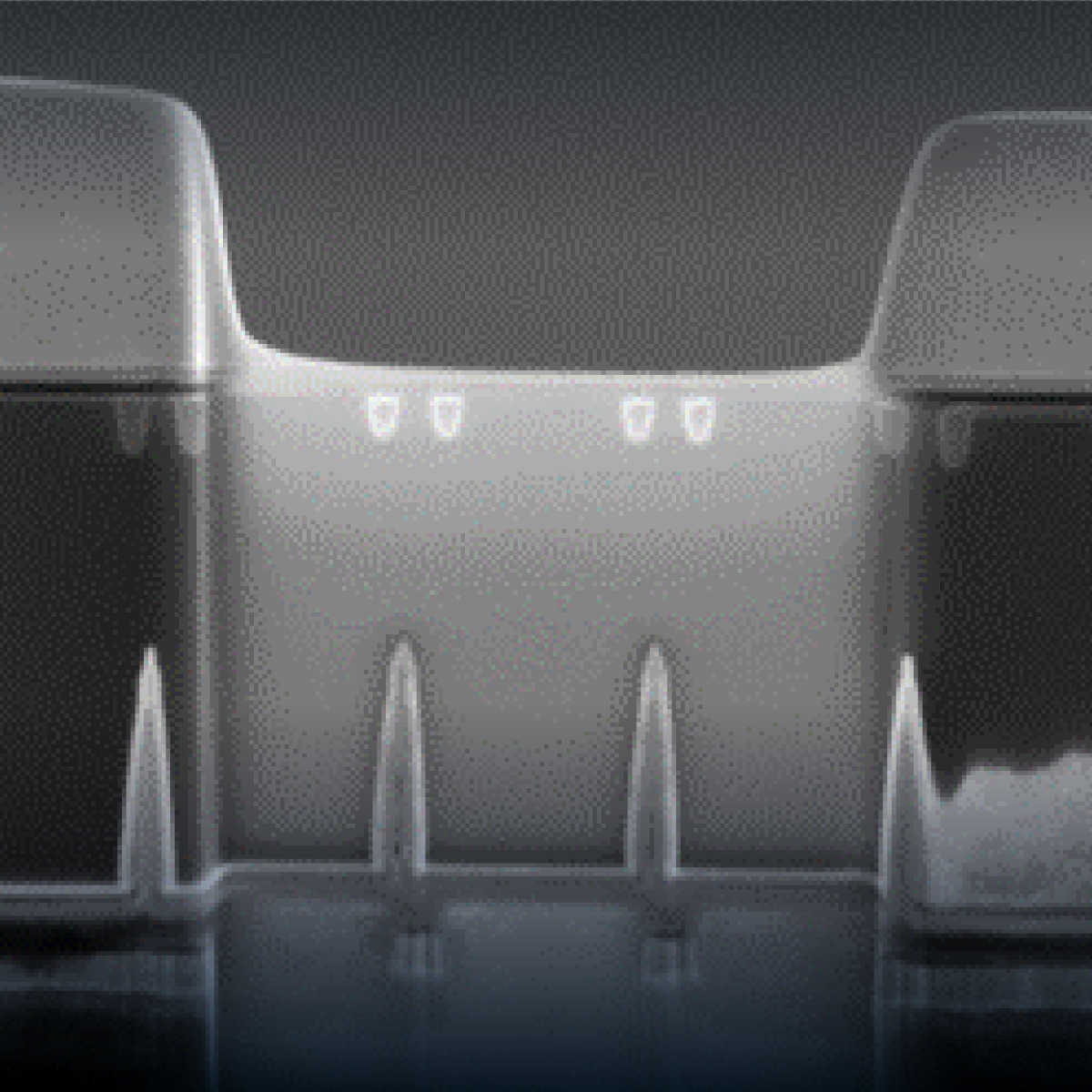
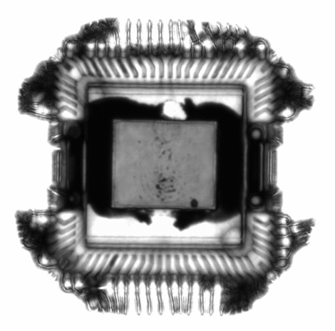
HAADF (High-Angle Annular Dark Field) STEM image of a MiM (Metal – Insulator – Metal) capacitor structure within an integrated circuit.
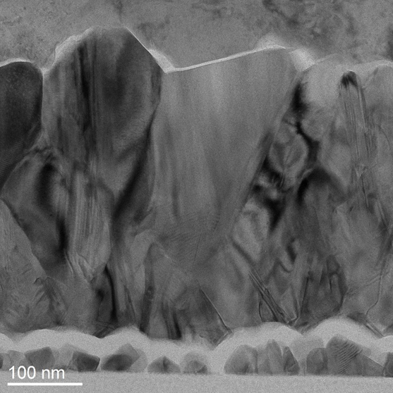
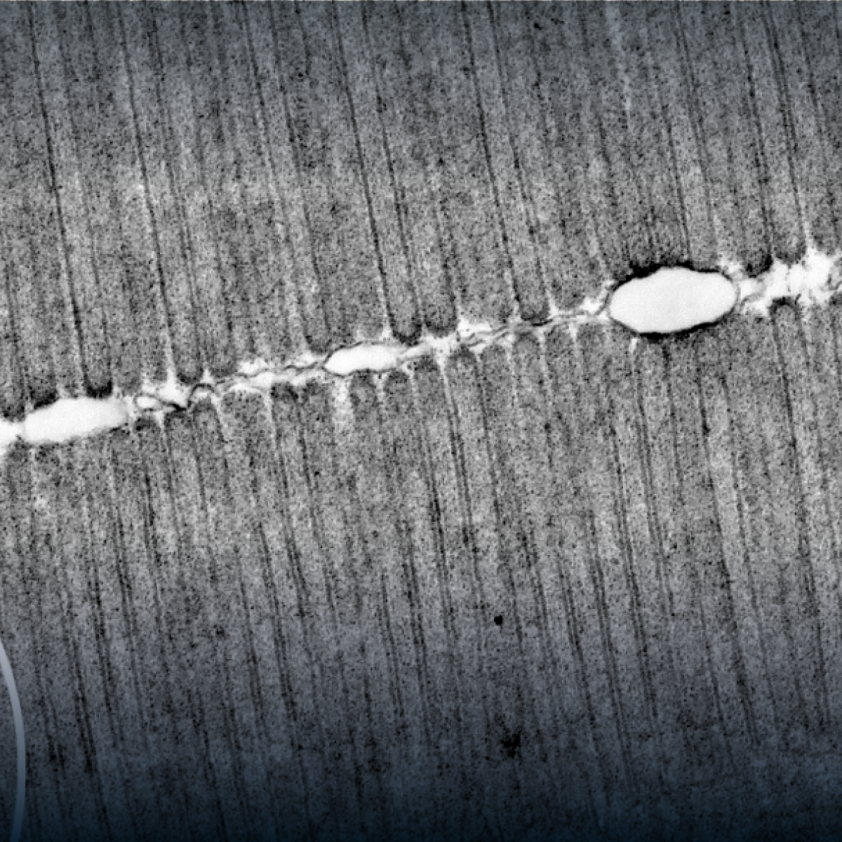
TEM micrograph capturing the interface between two layers of distinct materials with various crystalline phases. This image was shot at 35kx magnification.
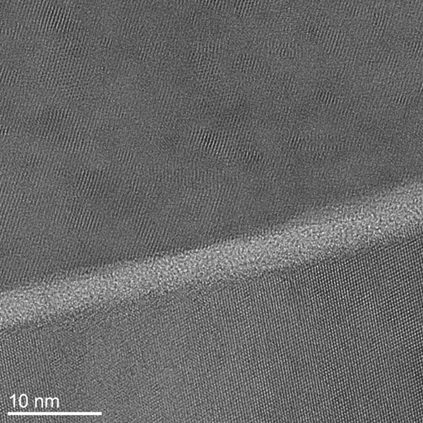
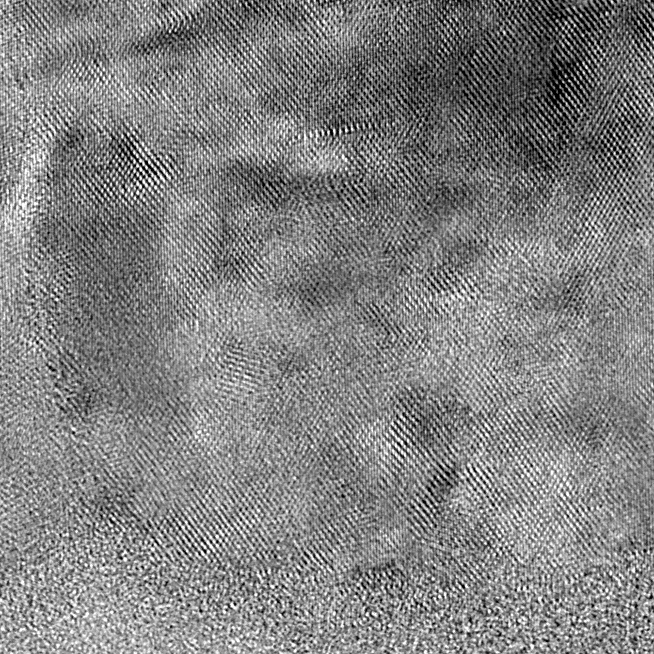
This TEM micrograph shows the same interface as above, captured at 410kx magnification. At this level of magnification, it is possible to see individual columns of atoms in within the crystalline domains of the materials.
Instruments Used for TEM
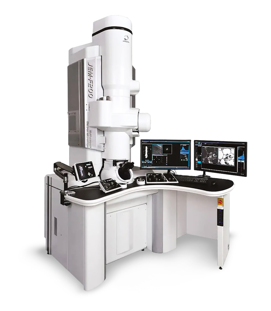
JEOL JEM-F200 Microscope
- Cold-Field-Emission Gun (CFEG) Electron Source
- Accelerating Voltage: 80 kV or 200 kV
- High current and beam stability = ultra-high spatial resolution
- TEM Point Resolution: 0.19 nm
- STEM-HAADF Resolution: 0.14 nm
- High Energy Resolution: 0.3 eV
- High-res Electron Energy Loss Spectroscopy (EELS)
- Fine Structure/Oxidation State Determination
- Plasmon Resonance Analysis (CFEG supports zero-loss peak)
- Gatan GIF Continuum ER Image Filter for Energy Filtered TEM (EFTEM) for light-element materials
- Dual SDD Energy Dispersive X-ray Spectroscopy (EDX/EDS) detectors
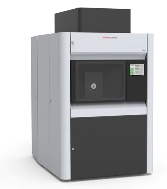
Thermo Scientific Talos F200X (S)TEM
- TEM Line Resolution: ≤ 0.10 nm
- TEM Information Limit: ≤ 0.12 nm
- Maximum Alpha Tilt: ± 90°
(with tomography holder) - Maximum Diffraction Angle: 24°
- Electron Source: High-Brightness Field Emission Gun
- Gatan OneView CCD: 16MP 4K camera
- Quad-EDS Detectors for enhanced sensitivity and detection limits
How TEM Works
In a TEM, a high-energy electron beam is applied to a very-thin sample (a lamella), which is prepared to be electron-transmissive i.e. typically 20 to 50 nm thick.
As the beam passes through the sample, scattering interactions occur between its electrons and the atoms present which alter the transmitted beam intensity. These scattering events can produce several types of contrast in the final image, including: amplitude contrast (arising from atomic number and mass/thickness) phase contrast (from quantum phase shifting due to multiple scattered beams’ interference), diffraction contrast (from crystal structure and orientation), and more.
Different imaging modes on the TEM can target certain types of contrast over others, facilitating specialized analysis of relevant information.
The electron beams transmitted through the sample are focused by the TEM objective lens to form an image below it. This image is then magnified through a final series of electromagnetic optics, and detected by a specialized CCD camera.
Additional Resources

4 Targets for Optimization in a Battery Cell
IN Publications
July 22, 2022

Batteries Industry Solutions
IN Publications
June 13, 2022
eBook: The Age of (Scanning) Transmission Electron Microscopy...
IN Publications
June 8, 2022
Key Principles of Lamella Sample Preparation for Transmission...
IN Publications
April 25, 2022
(Scanning) Transmission Electron Microscopy (S/TEM) Using the Thermo...
IN Publications
April 24, 2022
Electron and Ion Beam Imaging with DualBeam Focused...
IN Publications
April 22, 2022
(Scanning) Transmission Electron Microscopy Services
IN Publications
July 21, 2021
Choosing the Right Surface Imaging Technique
IN Publications
May 10, 2021

7 Myths About Modern TEM
IN Publications
April 21, 2021
+
Add to Comparison
Focused Ion Beam Scanning Electron Microscopy (FIB-SEM)
In Microscopy & Imaging
FIB-SEM systems are used to produce 2D and 3D images of surface topography, and are able to resolve...
+
Add to Comparison
Scanning Electron Microscopy (SEM)
In Microscopy & Imaging
Scanning electron microscopy (SEM) is a surface imaging technique capable of achieving nm resolution on topographical features. Additionally,...
+
Add to Comparison
Scanning Transmission Electron Microscopy (STEM)
In Microscopy & Imaging
STEM is a hybrid electron microscopy technique used for imaging and morphological characterization with atomic-scale resolution. In Covalent's...
+
Add to Comparison
Scanning Acoustic Microscopy (SAM)
In Microscopy & Imaging
Scanning Acoustic Microscopy (SAM) is a non-destructive and non-invasive imaging technique which uses ultrasound signals to visualize the...
✕
Comparison link sent successfully
✕
Please use valid email address
✕
You need to have at least 2 techniques to compare
✕
You can select maximum 5 techniques
