Attenuated Total Reflectance (ATR)
$99 Base price View My Quote RequestFocused Ion Beam Scanning Electron Microscopy (FIB-SEM)
This technique supports Live View
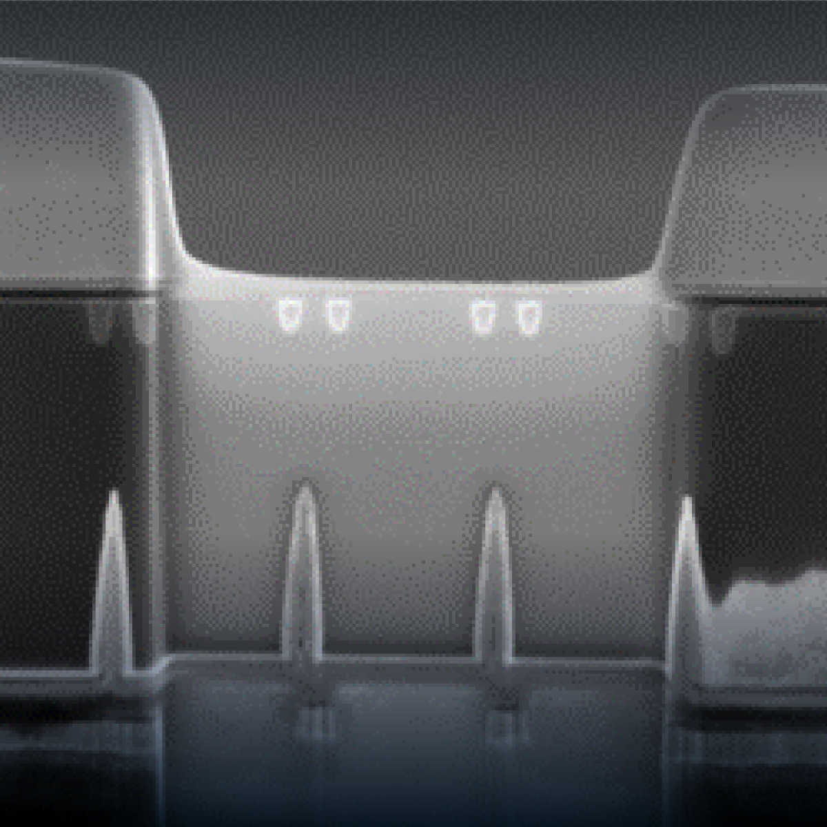
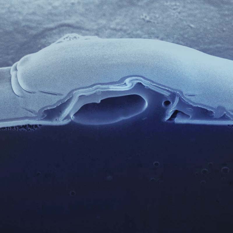
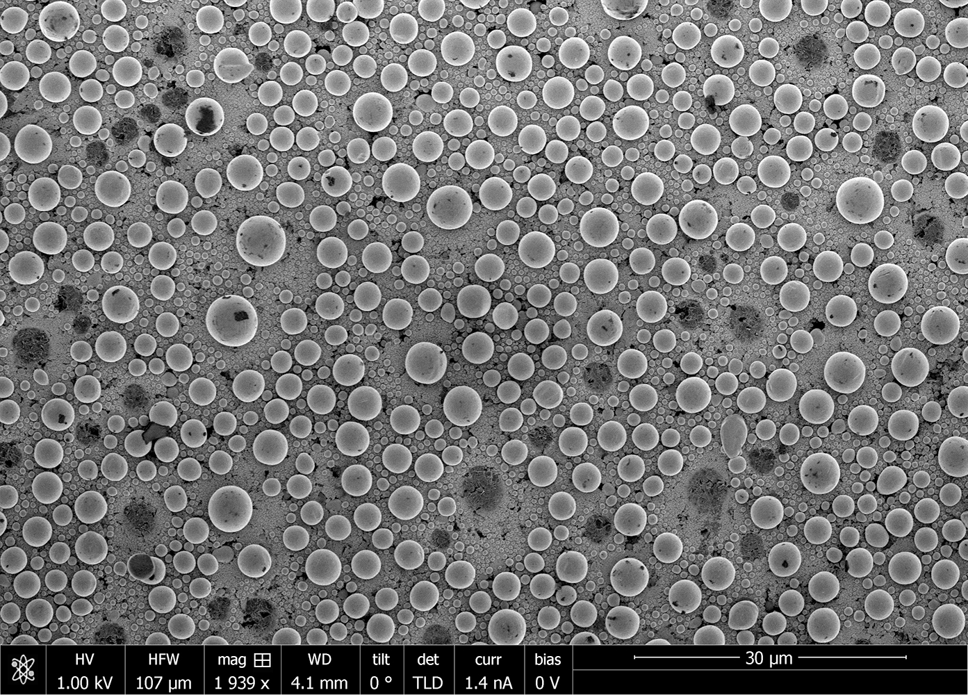
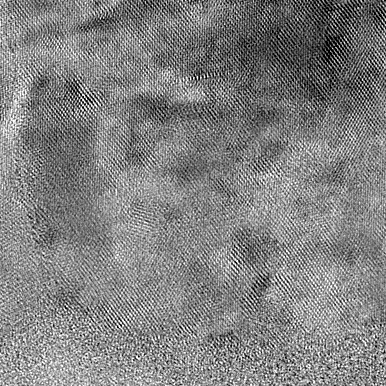
Like other high-resolution scanning electron microscopes, Focused-ion-beam scanning electron microscopes (FIB-SEMs) are used to produce 2D and 3D images of surface topography, and are able to resolve nm-scale features on a sample surface.
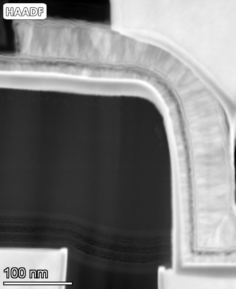
The FIB allows advanced analytical workflows such as: cross-section, tomography, lithography, lamella prep, and many others.
Strengths
- Ultra-high resolution imaging capabilities (limit resolution is < 1 nm)
- Able to image multi-modal, sub-surface, and 3D information
- FIB enables precise manipulation of sample in-situ: cutting, cleaving, trenching, exposing, and ion-welding of different fragments on the sample for imaging and analysis
Limitations
- Analysis is destructive
- Insulating materials impair precision of ion beam action and reduce imaging resolution
Technical Specifications:
Learn More:
Instruments Used for FIB-SEM
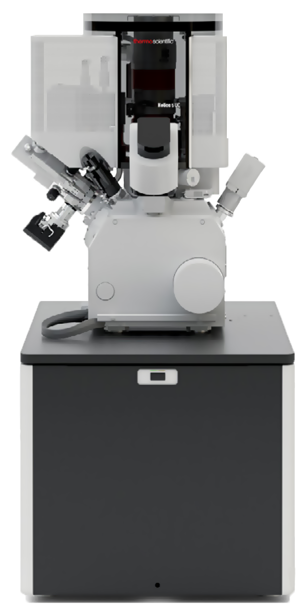
Thermo Scientific Helios 5 DualBeam
- Maximum Horizontal Field Width: 2.3 mm at 4 mm WD
- Electron Beam:
- Resolution Limit: 0.7 nm at 1 kV
- Current Range: 0.8 pA to 100 nA
- Accelerating Voltage Range: 350 V to 30 kV
- Ion Beam:
- Electron Beam:
- Resolution Limit: 4.0 nm at 30 kV using preferred statistical method
- Current Range: 1 pA to 100 nA
- Accelerating Voltage Range: 500 V to 30kV
- View Instrument Spec Sheet
Thermo Scientific Scios DualBeam
Optimized to achieve best performance across a wide array of sample types.
- Powerful charge neutralization
- Enables analysis on magnetic samples
- Able to operate above vacuum pressure
How FIB-SEM Works
On a FIB-SEM, the added focused-ion-beam allows for in situ sample manipulation. Normally the FIB beam is used to cross-section the sample at a precise location, but it can accomplish many other tasks such as: tomography, lithography, lamella prep, and more.
The imaging capabilities of the scanning-electron-beam in a FIB-SEM work as they do in any other SEM: the system generates an image by detecting electrons scattered by a highly-focused, high-energy applied electron beam as it is raster-scanned over the surface of a sample.
The secondary focused-ion-beam is comprised of high-energy, charged atoms (most commonly Ga+). When applied to the sample, the FIB can be tuned to either ablate material from the surface, or deposit atoms of an accompanying neutral gas.
Additionally, both in-house FIB-SEM instruments at Covalent also incorporate energy dispersive spectroscopy (EDS) detectors that enable measurement and mapping of elemental composition alongside all other FIB-SEM operations.
Additional Resources

4 Targets for Optimization in a Battery Cell
IN Publications
July 22, 2022

Batteries Industry Solutions
IN Publications
June 13, 2022
Key Principles of Lamella Sample Preparation for Transmission...
IN Publications
April 25, 2022
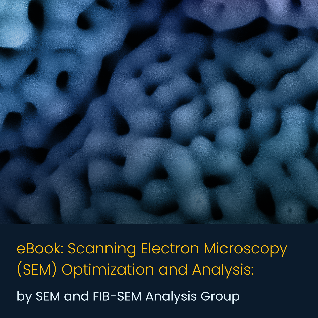
eBook: Scanning Electron Microscope (SEM) Optimization & Analysis
IN Publications
March 12, 2022
Examples of 3D Reconstruction with FIB-SEM Tomography
IN Publications
September 1, 2021
Scanning Electron Microscopy with Focused Ion Beam Services
IN Publications
July 21, 2021
3 Scanning Electron Microscopy (SEM) Signals You Need...
IN Publications
June 30, 2021

Datasheet: Medical Device Characterization with the Covalent Platform
IN Publications
June 14, 2021
Choosing the Right Surface Imaging Technique
IN Publications
May 10, 2021
+
Add to Comparison
Scanning Electron Microscopy (SEM)
In Microscopy & Imaging
Scanning electron microscopy (SEM) is a surface imaging technique capable of achieving nm resolution on topographical features. Additionally,...
+
Add to Comparison
Scanning Transmission Electron Microscopy (STEM)
In Microscopy & Imaging
STEM is a hybrid electron microscopy technique used for imaging and morphological characterization with atomic-scale resolution. In Covalent's...
+
Add to Comparison
Transmission Electron Microscopy (TEM)
In Microscopy & Imaging
TEM is the highest-resolution imaging technique available today. It is used to visualize sample features with atomic-level spatial...
+
Add to Comparison

Laser Scanning Confocal Microscopy (LSCM)
In Microscopy & Imaging
Laser scanning confocal microscopy (LSCM) is a nondestructive technique which generates 2D and 3D images of a sample...
✕
Comparison link sent successfully
✕
Please use valid email address
✕
You need to have at least 2 techniques to compare
✕
You can select maximum 5 techniques
