Attenuated Total Reflectance (ATR)
$99 Base price View My Quote RequestScanning Transmission Electron Microscopy (STEM)
Scanning transmission electron microscopy (STEM) is a hybrid electron microscopy technique used for imaging and morphological characterization with atomic-scale resolution.
STEM is available on both Covalent’s FIB-SEM instruments, as well as our TEM. All Covalent’s (S)TEM systems are additionally equipped with fully integrated energy-dispersive x-ray spectrometers (EDS or EDX) to allow correlative elemental composition and mapping analysis.
Strengths
- Atomic-level resolution limit – substantially improved over conventional SEM
- Enables spatial correlation of advanced TEM signals: EDS, EELS, Annular BF and DF scattered beams
Limitations
- Requires extensive sample preparation to generate a thin-enough analytical window for the material to be electron-transmissive
- High-energy, highly-focused electron beam can cause sample damage
Technical Specifications:
Learn More:
Example Outputs
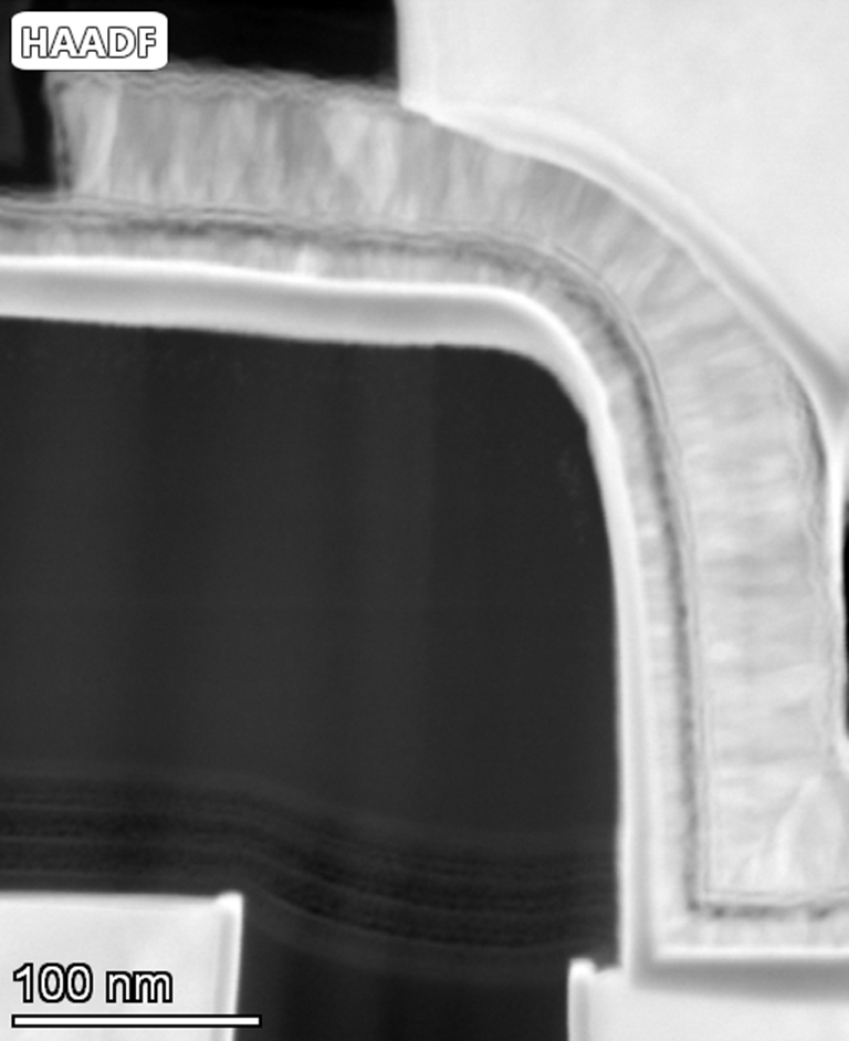
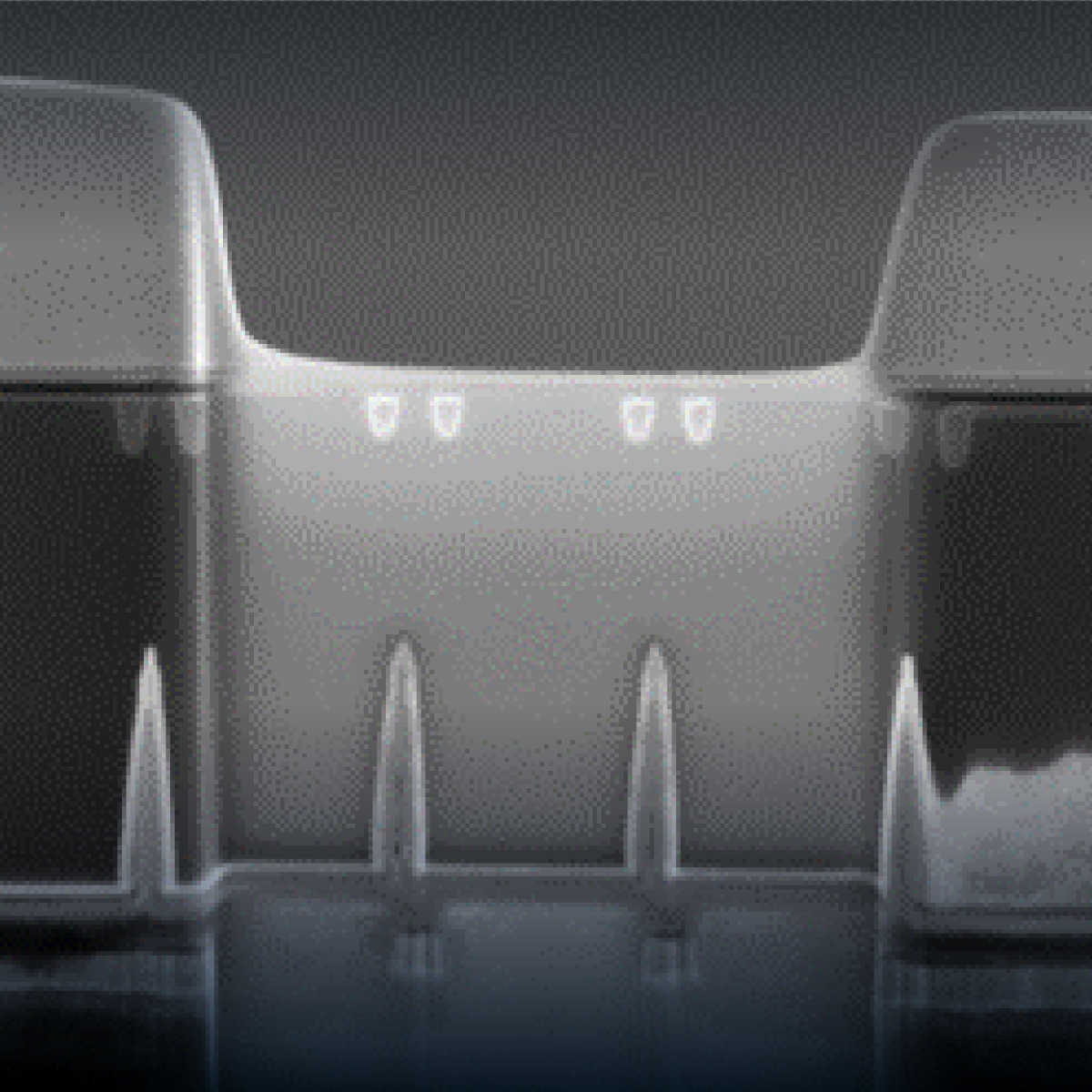
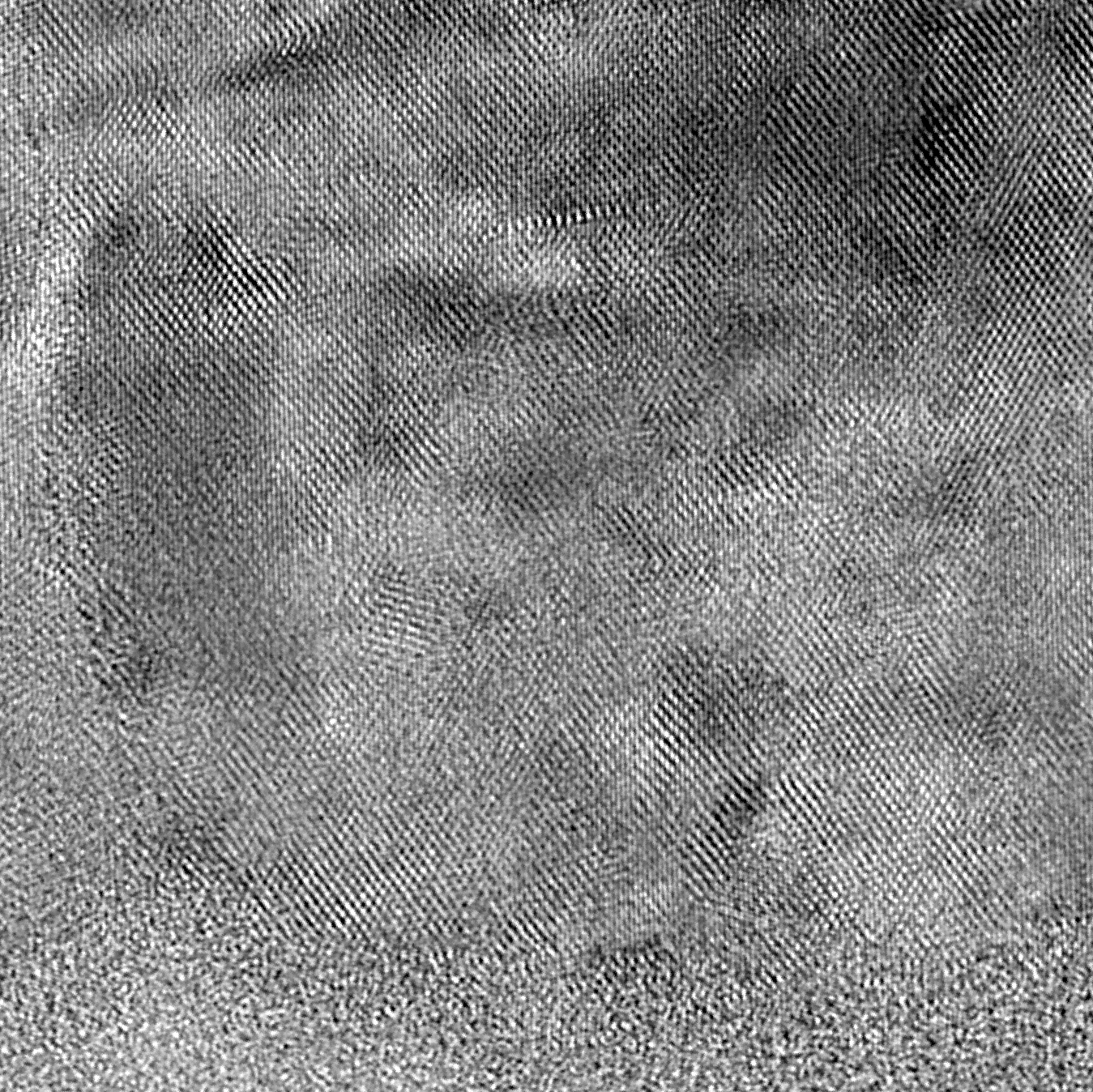
High angle annular dark-field (HAADF) TEM image captured at an ROI for joint analysis with EDS.
(S)TEM Bright-Field image of an interface between two layers, captured at 900kx magnification.

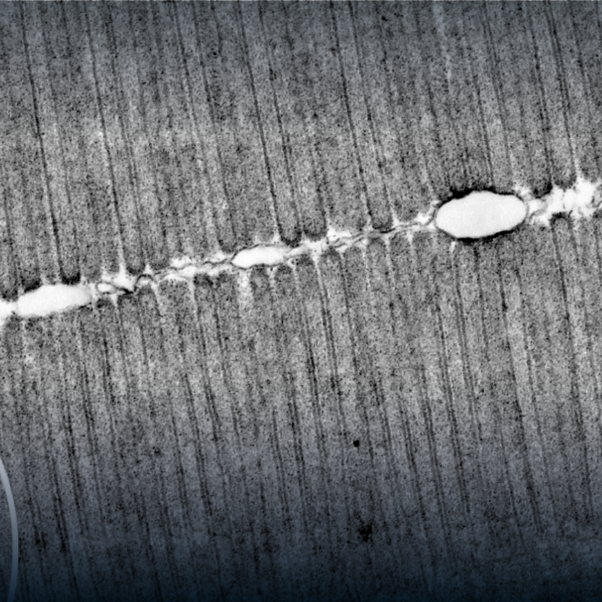
Energy dispersive spectroscopy (EDS) map of element distribution across the interface imaged above. This image is a composite overlay of the measured signal intensities of 9 different elements.
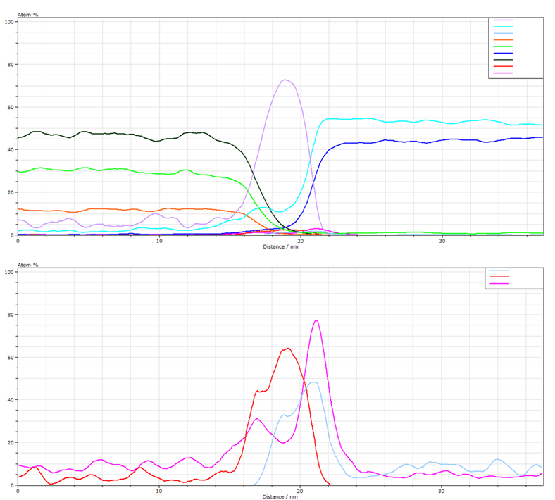
In addition to EDS maps, one can extract 2D line-scans of element concentration (in atomic %) across interfaces or boundaries between phase domains. These line scans were taken from across the same interface pictured previously. Top plot shows the measured intensities of all detected elements; bottom shows the interfacial diffusion of a selected 3 trace species.
Instruments Used for STEM
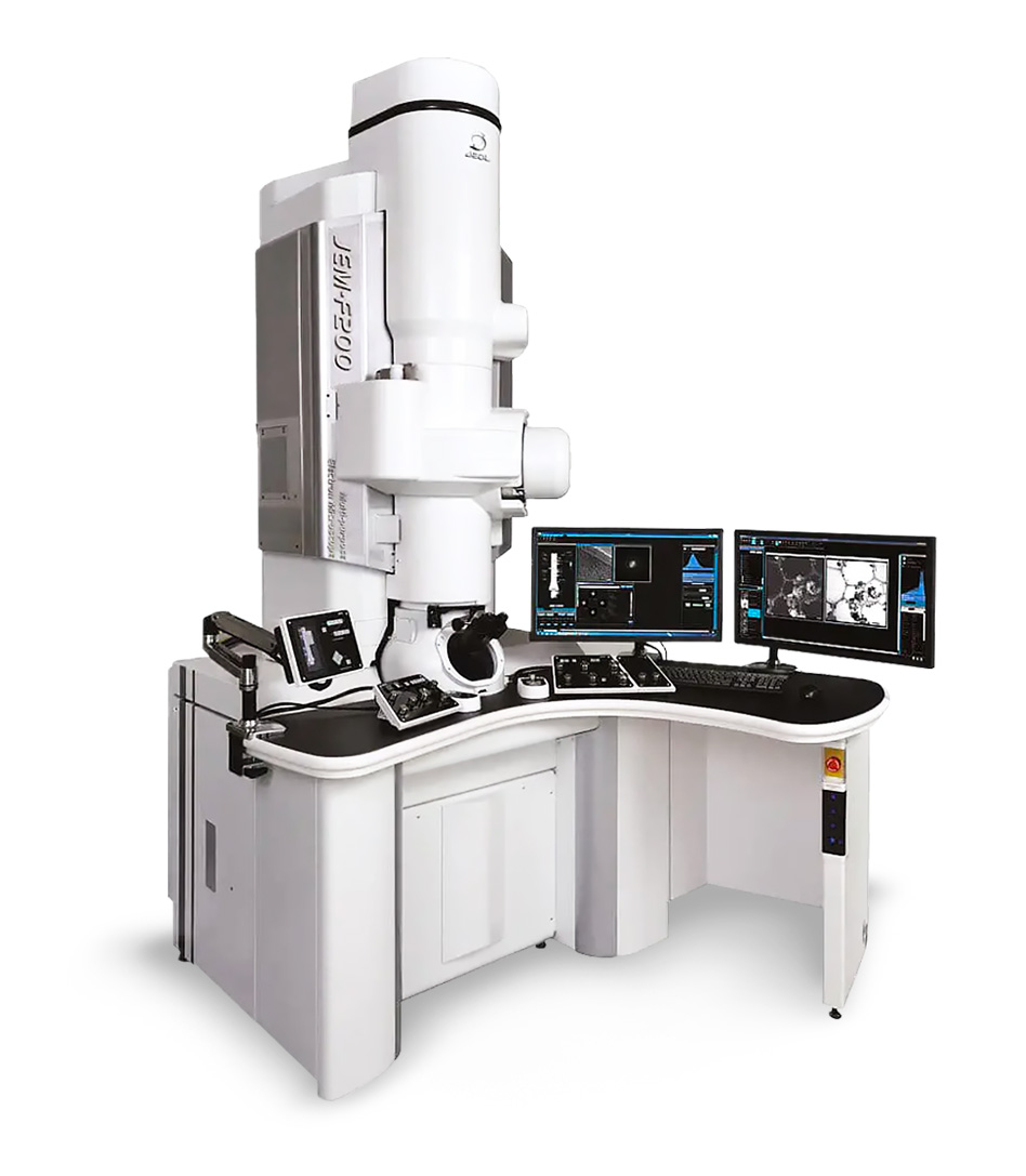
JEOL JEM-F200 Microscope
- Cold-Field-Emission Gun (CFEG) Electron Source
- Accelerating Voltage: 80 kV or 200 kV
- High current and beam stability = ultra-high spatial resolution
- TEM Point Resolution: 0.19 nm
- STEM-HAADF Resolution: 0.14 nm
- High Energy Resolution: 0.3 eV
- High-res Electron Energy Loss Spectroscopy (EELS)
- Fine Structure/Oxidation State Determination
- Plasmon Resonance Analysis (CFEG supports zero-loss peak)
- Gatan GIF Continuum ER Image Filter for Energy Filtered TEM (EFTEM) for light-element materials
- Dual SDD Energy Dispersive X-ray Spectroscopy (EDX/EDS) detectors
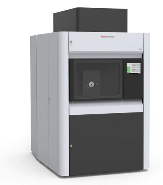
Thermo Scientific Talos F200X (S)TEM
- STEM Resolution Limit: 0.16 nm
(in High-Angle Annular Dark Field – HAADF – mode) - STEM Detectors:
- HAADF
- On-Axis Bright Field
- On-Axis Dark Field
- Maximum Alpha Tilt: ± 90°
(with tomography holder) - Maximum Diffraction Angle: 24°
- Electron Source: High-Brightness Field Emission Gun
- Maximum Horizontal Field Width: 2.3 mm at 4 mm WD
- Electron Beam:
- Resolution Limit: 0.7 nm at 1 kV
- Current Range: 0.8 pA to 100 nA
- Accelerating Voltage Range: 350 V to 30 kV
- Ion Beam:
- Electron Beam:
- Resolution Limit: 4.0 nm at 30 kV using preferred statistical method
- Current Range: 1 pA to 100 nA
- Accelerating Voltage Range: 500 V to 30kV
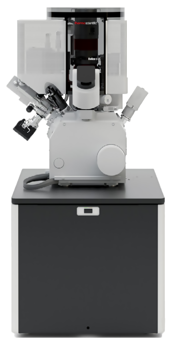
Thermo Scientific Scios DualBeam
Optimized to achieve best performance across a wide array of sample types.
- Powerful charge neutralization
- Enables analysis on magnetic samples
- Able to operate above vacuum pressure
How STEM Works
Like SEM systems, STEM instruments use a narrow, focused electron beam spot to probe the sample, scanning it in a raster pattern over an analytical area of interest. The output image is produced by detecting the scattered signal intensity at each pixel as the beam scans.
In a STEM – as in a TEM – the detector is mounted underneath the sample and picks up electrons which are transmitted through it. As such, STEM can only be used when the sample is sufficiently thin to be electron-transmissive.
In Covalent’s (S)TEM-enabled instruments, STEM offers improved spatial resolution compared to an SEM, and improved spatial correlation (for element mapping) compared to normal TEM.
Additional Resources
4 Targets for Optimization in a Battery Cell
IN Publications
July 22, 2022

Batteries Industry Solutions
IN Publications
June 13, 2022
eBook: The Age of (Scanning) Transmission Electron Microscopy...
IN Publications
June 8, 2022
Key Principles of Lamella Sample Preparation for Transmission...
IN Publications
April 25, 2022
(Scanning) Transmission Electron Microscopy (S/TEM) Using the Thermo...
IN Publications
April 24, 2022

Electron and Ion Beam Imaging with DualBeam Focused...
IN Publications
April 22, 2022
(Scanning) Transmission Electron Microscopy Services
IN Publications
July 21, 2021
Choosing the Right Surface Imaging Technique
IN Publications
May 10, 2021

7 Myths About Modern TEM
IN Publications
April 21, 2021
+
Add to Comparison
Transmission Electron Microscopy (TEM)
In Microscopy & Imaging
TEM is the highest-resolution imaging technique available today. It is used to visualize sample features with atomic-level spatial...
+
Add to Comparison
Scanning Electron Microscopy (SEM)
In Microscopy & Imaging
Scanning electron microscopy (SEM) is a surface imaging technique capable of achieving nm resolution on topographical features. Additionally,...
+
Add to Comparison
Scanning Acoustic Microscopy (SAM)
In Microscopy & Imaging
Scanning Acoustic Microscopy (SAM) is a non-destructive and non-invasive imaging technique which uses ultrasound signals to visualize the...
✕
Comparison link sent successfully
✕
Please use valid email address
✕
You need to have at least 2 techniques to compare
✕
You can select maximum 5 techniques
