Attenuated Total Reflectance (ATR)
$99 Base price View My Quote RequestEmission Microscopy (EMMI)
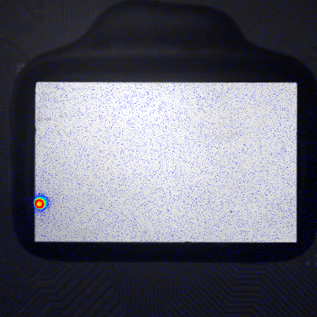
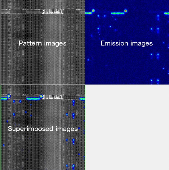
Emission Microscopy (EMMI) is a non-invasive and non-destructive optical analysis technique used to localize photon emissions from fault points on integrated circuits. It is the industry-leading failure analysis technique used to isolate and analyze particular electrical failure types, such as: defective or leaky semiconductor junctions, ESD-induced damage, latch-up, and leakage current or overcurrent, among others.
Strengths
- Efficient detection and localization of integrated circuit electrical failures
- Non-invasive and non-destructive
- Viable for both wire bonded and flip-chip devices
Limitations
- Ohmic and metallic short-circuits are not well suited for EMMI analysis
- We offer infrared thermographic imaging as well as liquid crystal hot spot detection techniques for this class of failures.
- 100% visibly obscured failure sites on the sample cannot be analyzed
- (NOTE: sites on the die with typical metallization/traces can be analyzed; however, emissions from sites that are masked by expansive metal will be difficult to detect)
Technical Specifications:
Learn More:
Sample Requirements
- Semiconductor devices
- At this time, we cannot support wafers due to lack of internal probe station
- Samples requiring fine probing are not well suited for this analysis – contact us to learn more
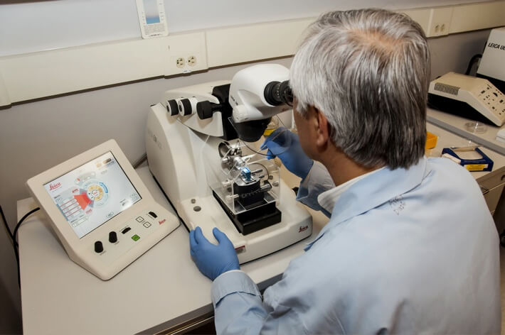
How EMMI Works
EMMI, also called Photon Emission Microscopy (PEM) or Light Emission Microscopy (LEM), is able to detect emissions from electrical fail-points from either the front or backside (“flip-chip”) of silicon devices.
The analysis requires a highly sensitive camera (CCD or InGaAs detector) to capture photon emissions from localized failure sites on integrated circuits. The detected photons are emitted when electron-hole pairs are recombined within the analyzed area of the circuit.
Signals from EMMI can be difficult to interpret; experienced analysts are required to maximize the accuracy and impact of measurement. Covalent’s failure analysis team has over 100 years of collective experience in localizing semiconductor die failures and can support your project with the necessary depth of expertise.
+
Add to Comparison

Infrared Thermography (IRT)
In Analytical Services
Infrared thermography can be used to measure the heat distribution in integrated circuits (die) and printed circuit boards,...
+
Add to Comparison
Emission Microscopy (EMMI)
In Analytical Services
Emission Microscopy (EMMI) is a non-invasive and non-destructive optical analysis technique used to localize photon emissions from fault...
✕
Comparison link sent successfully
✕
Please use valid email address
✕
You need to have at least 2 techniques to compare
✕
You can select maximum 5 techniques
