Attenuated Total Reflectance (ATR)
$99 Base price View My Quote RequestDye & Pry Testing (Dye & Pry)
Dye and Pry testing is a destructive, IPC-prescribed failure-analysis and quality-control technique performed on solder joints on printed circuit board assemblies (PCBA) to identify certain defects unique to solder joints, such as: cracks, “head-in-pillow” defects, and other joint separations.
Even when compared against X-ray analytical techniques, ‘Dye and Pry’ remains the most widely accepted technique for characterizing solder-ball die-attach quality defects.
Our technical experts have over 20 years of experience executing Dye & Pry analysis in accordance with IPC standards.
Strengths
- Best known method for identifying solder-joint defects on a BGA device
- All solder joints on a BGA are tested simultaneously
- Able to characterize fine cracks and cratering that are invisible to X-ray systems
- Robust documentation and compliance standards available
Limitations
- Destructive analysis: typically, samples used in Dye & Pry testing are not suitable for subsequent analysis with other techniques
- Extensive expertise required to optimize sample preparation for accurate, complete analysis
Technical Specifications:
Learn More:
Example Outputs
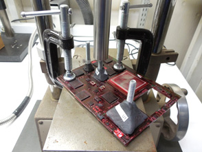
PCB assembly after red dye and bake-out. A hex bolt is attached to the device under test using a special epoxy putty and/or adhesive. The board is clamped to the stage and the device is pulled straight up so that no artifacts are introduced.
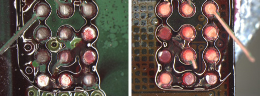
Board side (Left) and component side (Right) showing solder joint cracks at the board Intermetallic (IMC) layer and board pad lifts (cratering). Fractured BGA solder joints are a Defect per IPC-A-610G, section 8.3.12. Lifted Lands (Pad Cratering) is a defect per IPC-A-610G, section 10.3.2.
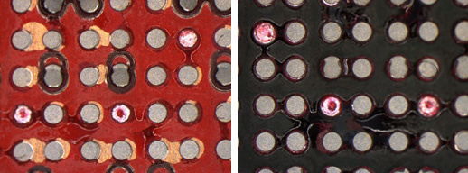
Board side (Left) and component side (Right) showing 3 solder joints with a smooth dome marked by red dye, indicating “Head in Pillow” defects. These (non-continuous) solder joints are Defects per IPC-A-610G, section 8.3.12.
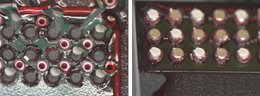
Board side (Left) and component side (Right) showing no pre-existing cracks or other separations. The dye adheres to the solder balls and the solder mask windows in the board but does not penetrate the joints. These BGA solder joints are Acceptable from Dye & Pry per IPC-A-610G, section 8.3.12.
How Dye & Pry Works
Dye an Pry procedures begin by submerging a target board in a specialized red, blue or green fluorescent dye, using vacuum-pressure impregnation. The marker fluid penetrates any cracks or other openings in the exposed solder joints. As part of this process, a final bake-out is done to set the dye. After bake-out, a pulling jig (which can sometimes be as simple as a hex bolt) is bonded to the top surface of the attached component using epoxy.
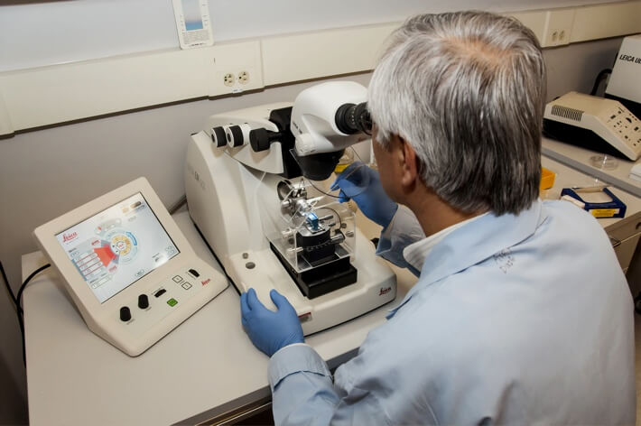
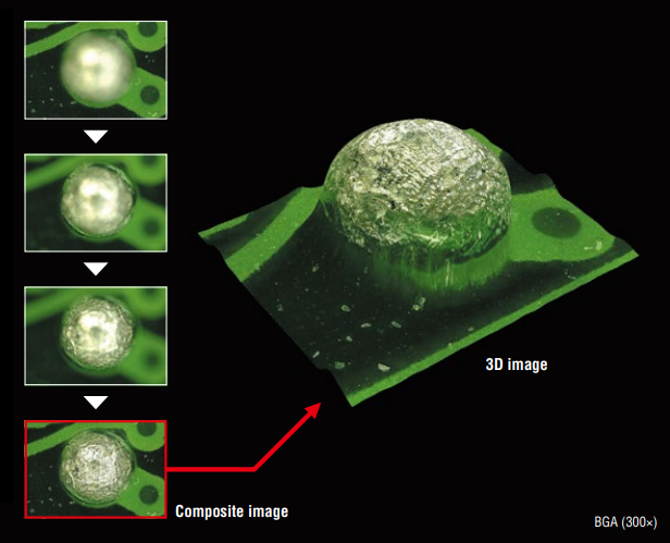
Once the epoxy is set, the components are manually pulled from the board to allow visual assessment of the solder joints. Any pre-existing cracks will be stained red. Each joint is then inspected at a minimum 40X magnification using Advanced Optical Microscopy.
Covalent provides a complete report of this analysis, which includes a selection of images captured of the total board and representative solder joints from planar (top-down) and lateral (side) orientations.
+
Add to Comparison
Digital Optical Microscopy (VH Microscope)
In Microscopy & Imaging
Optical microscopy is ubiquitous in diverse fields within academic research and commercial industries. It is an affordable, rapid...
+
Add to Comparison
IPC Compliance Testing
In Failure Analysis
IPC Compliance testing via destructive physical analysis provides a comprehensive screening for quality assurance and comprises the best-known...
+
Add to Comparison
Mechanical Cross-Section Analysis
In Failure Analysis
Material cross section analysis enables one to expose buried features on a sample in a controlled fashion, to...
✕
Comparison link sent successfully
✕
Please use valid email address
✕
You need to have at least 2 techniques to compare
✕
You can select maximum 5 techniques
