Failure Analysis
When you encounter a problem or performance defect with your part or device, it can cause serious stalls in development and production. These delays cost you time and money, unnecessarily.
Working with a qualified Failure Analysis partner like Covalent can accelerate problem solving by infusing your team with actionable data and domain-specific expertise.
Our team has nearly a century of combined experience in helping teams like yours to:
- Identify failure mechanisms
- Improve production processes
- Enhance the reliability, performance, and consistency of products
14 techniques found in Failure Analysis
+
Add to comparison
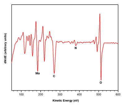
Auger Electron Spectroscopy (AES)
In Analytical Chemistry,Microscopy & Imaging,Failure Analysis
Auger electron spectroscopy (AES) is a surface-sensitive analytical technique with high lateral resolution. It is used to quantify and map the elemental composition of the outermost 2-10 nm of a material.
+
Add to comparison
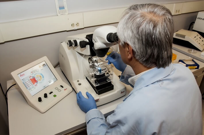
Digital Optical Microscopy (VH Microscope)
In Microscopy & Imaging,Failure Analysis
Optical microscopy is ubiquitous in diverse fields within academic research and commercial industries. It is an affordable, rapid analytical imaging technique used to visualize samples. While optical microscopes may be common, many instruments fall far short on performance when compared with the cutting-edge digital microscope systems available at Covalent.
+
Add to comparison
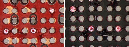
Dye & Pry Testing (Dye & Pry)
In Failure Analysis
Dye and Pry testing is a destructive, IPC-prescribed failure-analysis and quality-control technique performed on solder joints on printed circuit board assemblies (PCBA) to identify certain defects unique to solder joints, such as: cracks, “head-in-pillow” defects, and other joint separations. Even when compared against X-ray analytical techniques, 'Dye and Pry' remains the most widely accepted technique for characterizing solder-ball die-attach quality defects. Our technical experts have over 20 years of experience executing Dye & Pry analysis in accordance with IPC standards.
+
Add to comparison
Emission Microscopy (EMMI)
In Analytical Services,Microscopy & Imaging,Failure Analysis
Emission Microscopy (EMMI) is a non-invasive and non-destructive optical analysis technique used to localize photon emissions from fault points on integrated circuits. It is the industry-leading failure analysis technique used to isolate and analyze particular electrical failure types, such as: defective or leaky semiconductor junctions, ESD-induced damage, latch-up, and leakage current or overcurrent, among others.
+
Add to comparison
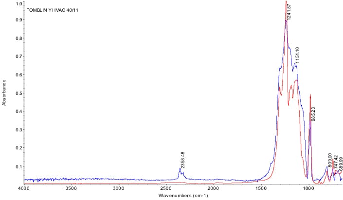
Fourier Transformed Infrared Spectroscopy (FTIR)
In Analytical Chemistry,Failure Analysis
Fourier-transformed infrared spectroscopy (FTIR) is a nondestructive, optical technique used to analyze chemical composition and the optical properties of a material.
+
Add to comparison
IPC Compliance Testing
In Failure Analysis
IPC Compliance testing and destructive physical analysis (DPA) provide a comprehensive screening for quality assurance and comprise the best-known method to identify design or production issues in electronics assemblies, components, and fabricated boards. This procedure includes a complete program of analytical methods and procedures for characterizing modern electronics boards.
+
Add to comparison
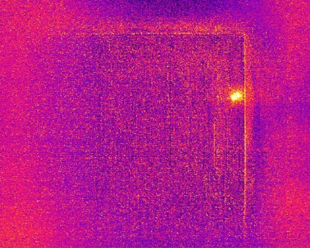
Infrared Thermography (IRT)
In Analytical Services,Microscopy & Imaging,Failure Analysis
Infrared thermography (IRT) is the leading non-invasive and non-destructive method used to detect and localize material defects, short circuits, and other powered failures. It works by analyzing the heat dissipation that results from these device faults. Infrared thermography can be used to measure the heat distribution in integrated circuits (die) and printed circuit boards, and nearly any powered device to detect hot spots.
+
Add to comparison
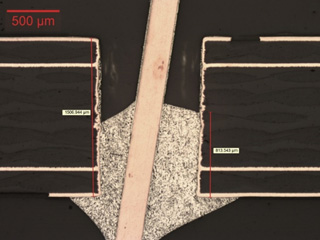
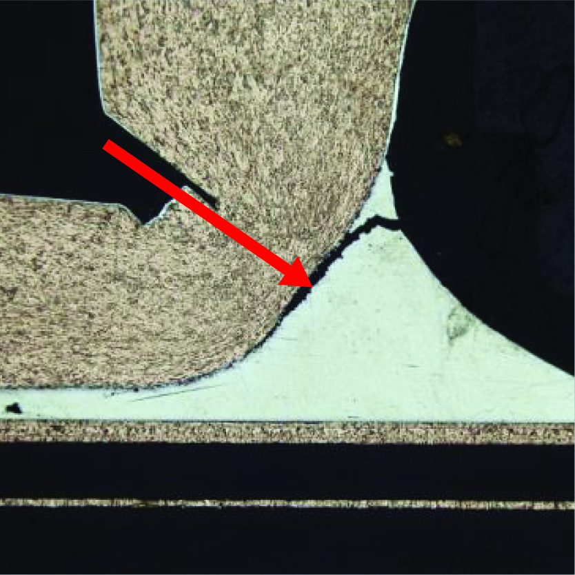
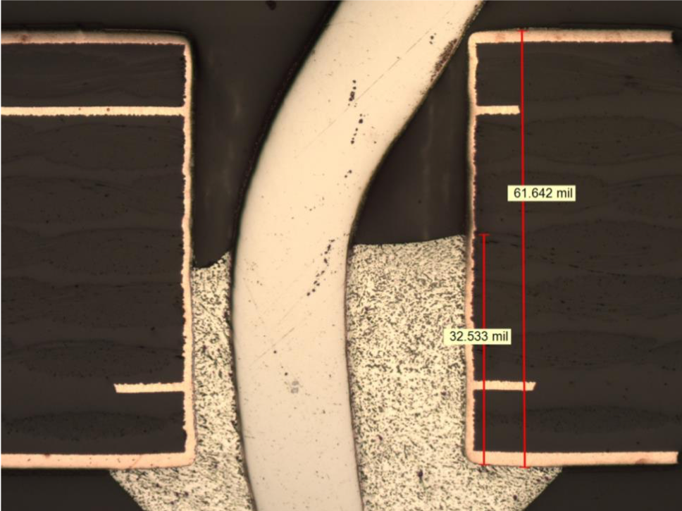
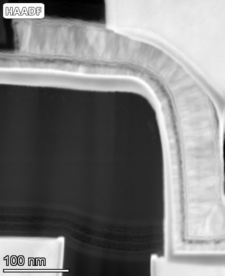
Mechanical Cross-Section Analysis
In Failure Analysis
Mechanical cross section analysis enables one to expose buried features on a sample in a controlled fashion. It is regularly used in IPC compliance testing, to assay critical dimensions, or to identify miscellaneous structural defects or abnormalities such as: cracks, bridging, delamination, deformations, and more. Covalent Metrology’s technical staff have over 30 years of experience in preparation and measurement of sample cross sections. In addition, our team is certified to conduct IPC qualified cross-sectional procedures for PCB failure analysis and quality control.
+
Add to comparison

Nanoindentation (Nano-Indent)
In Material Testing,Failure Analysis
Nanoindentation (nano-indent) is a quasi-static mode of nanomechanical analysis used to measure hardness and reduced elastic modulus of solid samples. It is especially useful for evaluating thin film coatings.
+
Add to comparison
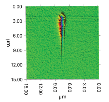
Nanomechanical Scratch Test (Nano-Scratch)
In Material Property Testing,Failure Analysis
Nanomechanical scratch testing (nano-scratch) is an alternate nanomechanical testing mode to nano-indent or nano-wear box testing, which is used to measure force response and mechanical properties typically of thin films and coatings.
+
Add to comparison
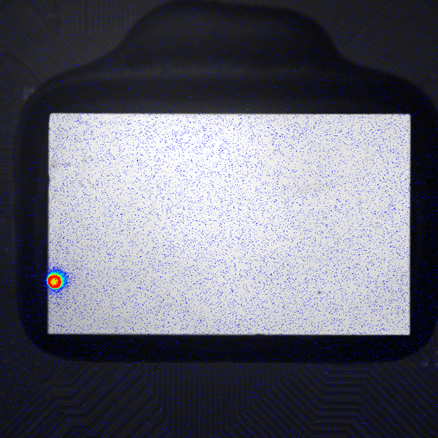
Near-infrared Imaging (NIR)
In Analytical Services,Microscopy & Imaging,Failure Analysis
Near-infrared imaging (NIR) is a nondestructive, noninvasive, and highly efficient method for localizing certain defects in photovoltaics and solar cells via electroluminescence. The technique is also a viable means of localizing defects in NIR fiber optic systems and lasers as well as monitoring high-temperature systems. NIR is currently seeing a growing field of application in pharmaceutical and polymers applications.
Technique Supports
+
Add to comparison
Scanning Acoustic Microscopy (SAM)
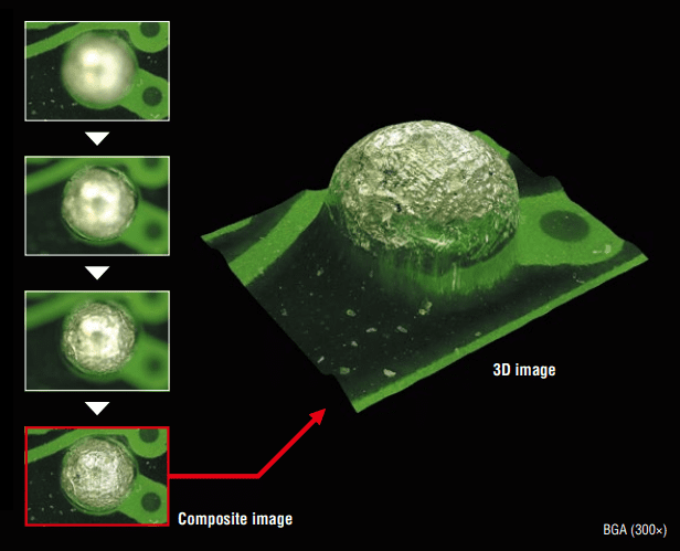
In Microscopy & Imaging,Failure Analysis
Scanning Acoustic Microscopy (SAM) is a non-destructive and non-invasive imaging technique which uses ultrasound signals to visualize the internal structures of a sample.
Techniques Showcase
Focused Ion Beam Scanning Electron Microscopy (FIB-SEM)
In Microscopy & Imaging
Base Price: $450 per Hour
FIB-SEM systems are used to produce 2D and 3D images of surface topography, and are able to resolve...
Nanoindentation (Nano-Indent)
In Material Testing,Failure Analysis
Base Price: $500 per Sample
Nanoindentation is a quasi-static mode of nanomechanical analysis used to measure hardness and reduced elastic modulus of solid...
Scanning Acoustic Microscopy (SAM)
In Microscopy & Imaging,Failure Analysis
Base Price: $450 per Sample
Scanning Acoustic Microscopy (SAM) is a non-destructive and non-invasive imaging technique which uses ultrasound signals to visualize the...
Scanning Transmission Electron Microscopy (STEM)
In Microscopy & Imaging,Particle Analysis
Base Price: $450 per Hour
STEM is a hybrid electron microscopy technique used for imaging and morphological characterization with atomic-scale resolution. In Covalent's...
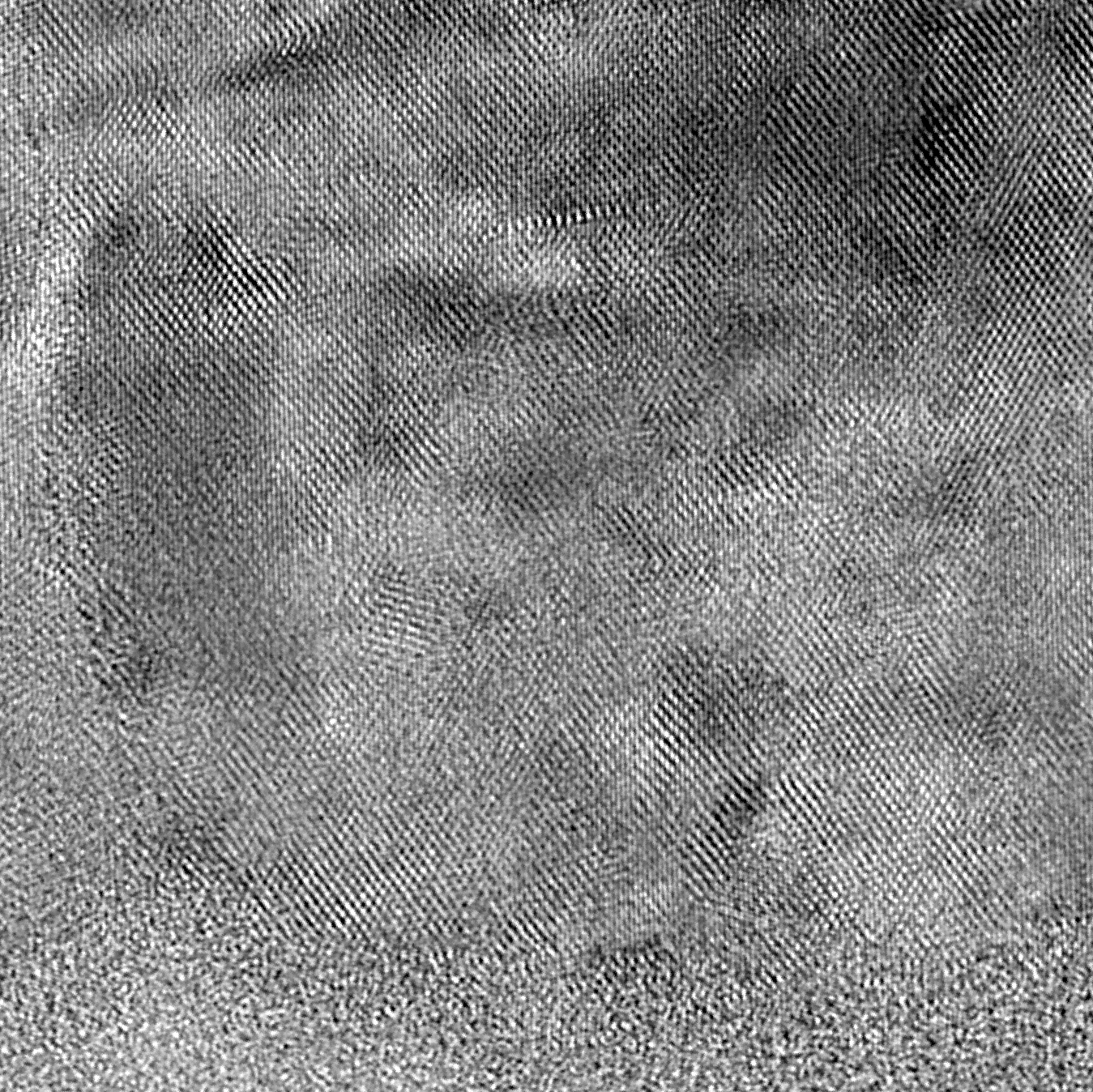
Transmission Electron Microscopy (TEM)
In Microscopy & Imaging,Particle Analysis
Base Price: $450 per Sample
TEM is the highest-resolution imaging technique available today. It is used to visualize sample features with atomic-level spatial...
Glow Discharge Optical Emission Spectroscopy (GDOES)
In Analytical Chemistry
Base Price: $375 per Hour
Glow discharge optical emission spectroscopy (GDOES) is a quantitative, chemical analytical technique used to study the elemental composition...

Inductively Coupled Plasma Mass Spectroscopy (ICP-MS)
In Analytical Services,Analytical Chemistry
please contact us for pricing
Inductively Coupled Plasma Mass Spectroscopy (ICP-MS) is a highly sensitive chemical analysis technique which measures the elemental composition...
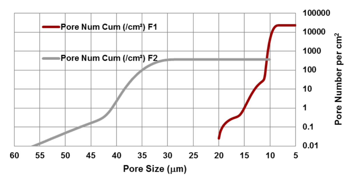
Capillary Flow Porometry (Porometry)
In Material Testing
please contact us for pricing
Capillary Flow Porometry (also called Porometry) is an optimal technique for characterizing through-pore size and size distribution.
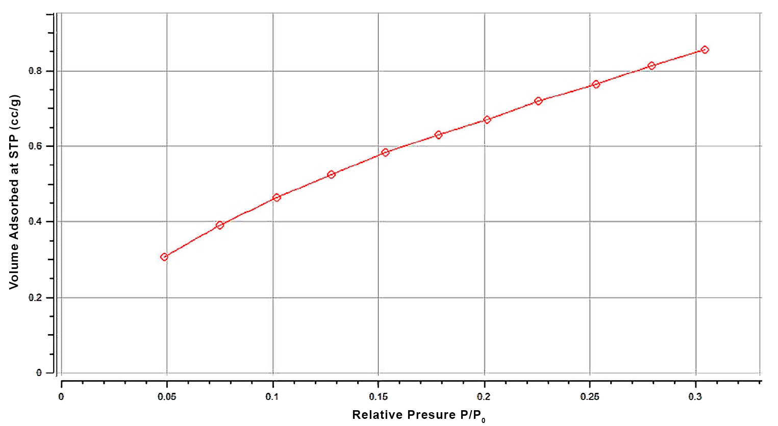
Porosimetry
In Material Testing
Base Price: $150 per Sample
Gas Adsorption Analysis is used for measuring specific surface area, pore sizes / size distribution, and overall porosity...
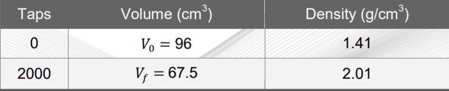
Tap Density Analysis
In Material Testing
Base Price: $175 per Sample
Tap Density Analysis provides fast, effective measurements of the bulk density of powders and establishes a quantitative metric...
Focused Ion Beam Scanning Electron Microscopy (FIB-SEM)
In Microscopy & Imaging
Base Price: $450 per Hour
FIB-SEM systems are used to produce 2D and 3D images of surface topography, and are able to resolve...

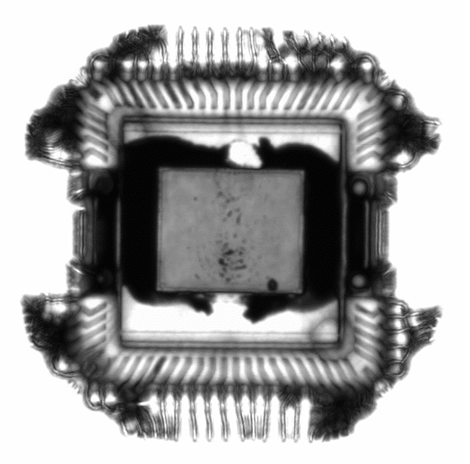
X-ray Computed Tomography (Micro-CT)
In Microscopy & Imaging,X-ray Analysis,Failure Analysis
Base Price: $400 per Hour
X-ray computed tomography (often referred to as Micro-CT due to its spatial resolution) is a non-contact, nondestructive 2D...
Nanoindentation (Nano-Indent)
In Material Testing,Failure Analysis
Base Price: $500 per Sample
Nanoindentation is a quasi-static mode of nanomechanical analysis used to measure hardness and reduced elastic modulus of solid...
✕
Comparison link sent successfully
✕
Please use valid email address
✕
You need to have at least 2 techniques to compare
✕
You can select maximum 5 techniques
