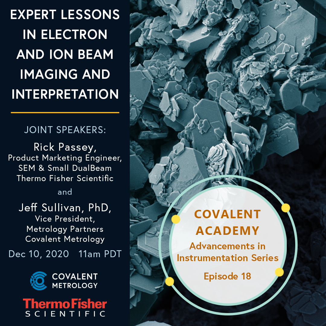
Expert Lessons in Electron and Ion Beam Imaging and Interpretation
In this webinar, our experts will discuss cutting-edge techniques and best practices for optimizing images captured with a FIB-SEM DualBeam microscope. Topics will include image interpretation, exploration of new state-of-the-art instrumentation, and the realm of analytical possibilities accessed using these techniques.
A DualBeam FIB-SEM combines a scanning electron microscope with a focused-ion-beam (FIB-SEM). With myriad detectors, the SEM produces nanometer-scale 2D images that interrogate different physical properties of the sample from topography to elemental composition to crystal structure. FIB imaging, while not as high-resolution as SEM imaging, offers another mode for extracting information from a sample. Additionally, the FIB allows for in situ sample alteration; it can be used to precisely cross-section, remove layers from, or mill arbitrary patterns into the sample. The FIB allows advanced analytical workflows such as: 3D slice-and view (tomography), subsurface cross-sectional characterization, and TEM lamella prep.
Application areas include metallurgy, semiconductors, nanomaterials, energy storage, medical devices, biotech, green energy, microelectronics and more.
Join the live event to learn more about:
1. Overview of FIB-SEM DualBeam systems
2. How to interpret images based on the contrast mechanisms, how to choose the contrast mechanism that highlights the phenomenon of interest, and how to set up the instrument to obtain that contrast mode
3. Troubleshooting methods for optimal microscope setup to obtain the desired images
4. Features, functions, and applications of instruments like the Thermo Scientific Scios & Helios 5
About the Speakers

Jeff Sullivan, PhD
Jeff’s career has focused on the technology-oriented product life cycle of both materials and capital equipment, from research and development through engineering, new product introduction, and manufacturing to customer adoption. With the General Electric (“GE”) Company from 2010 to 2017, Jeff was an Advanced R & D Leader at GE Global Research and Factory Integration Leader at GE Renewables. He held the roles of Director of Engineering, Senior Program Manager and Engineer Manager at Applied Materials, Inc. from 1999 to 2010. Jeff holds a PhD and Master of Science from the University of Wisconsin – Madison as well as a Bachelor of Arts from Grinnell College. He has been awarded more than fifteen United States patents in disciplines ranging from laser interferometry to photovoltaic manufacturing. Jeff is certified as a Green Belt and trained as a Master Black Belt in GE’s Lean/Six Sigma quality system.
Rick Passey
Rick Passey is an SEM/DualBeam applications expert who has been with Thermo Fisher Scientific (formerly FEI) for 12 years. His experience covers a wide range of microscopes and techniques, from environmental SEMs to the plasma FIB, 3D EDS/EBSD characterization to advanced TEM sample preparation. Prior to working with FEI, Rick spent 13 years as a Process Engineer with Hewlett Packard, leading an SEM/FIB laboratory, supporting materials characterization and failure analysis of inkjet and related technologies.
About Covalent Metrology
Covalent Metrology is a disruptive analytical services laboratory and platform based in Sunnyvale, California. Its mission is to help companies who use advanced materials to get better data and insights more easily and affordably to facilitate faster development and production. Covalent is dramatically changing the characterization and imaging landscape by combining transparent pricing, data platforms, and top-notch customer service with world-class scientists, state-of-art tools, and strategic partnerships.
Covalent now has over 500 customers in 20+ industries.
Learn more at: https://staging-covalentmetrologyproduction.kinsta.cloud
