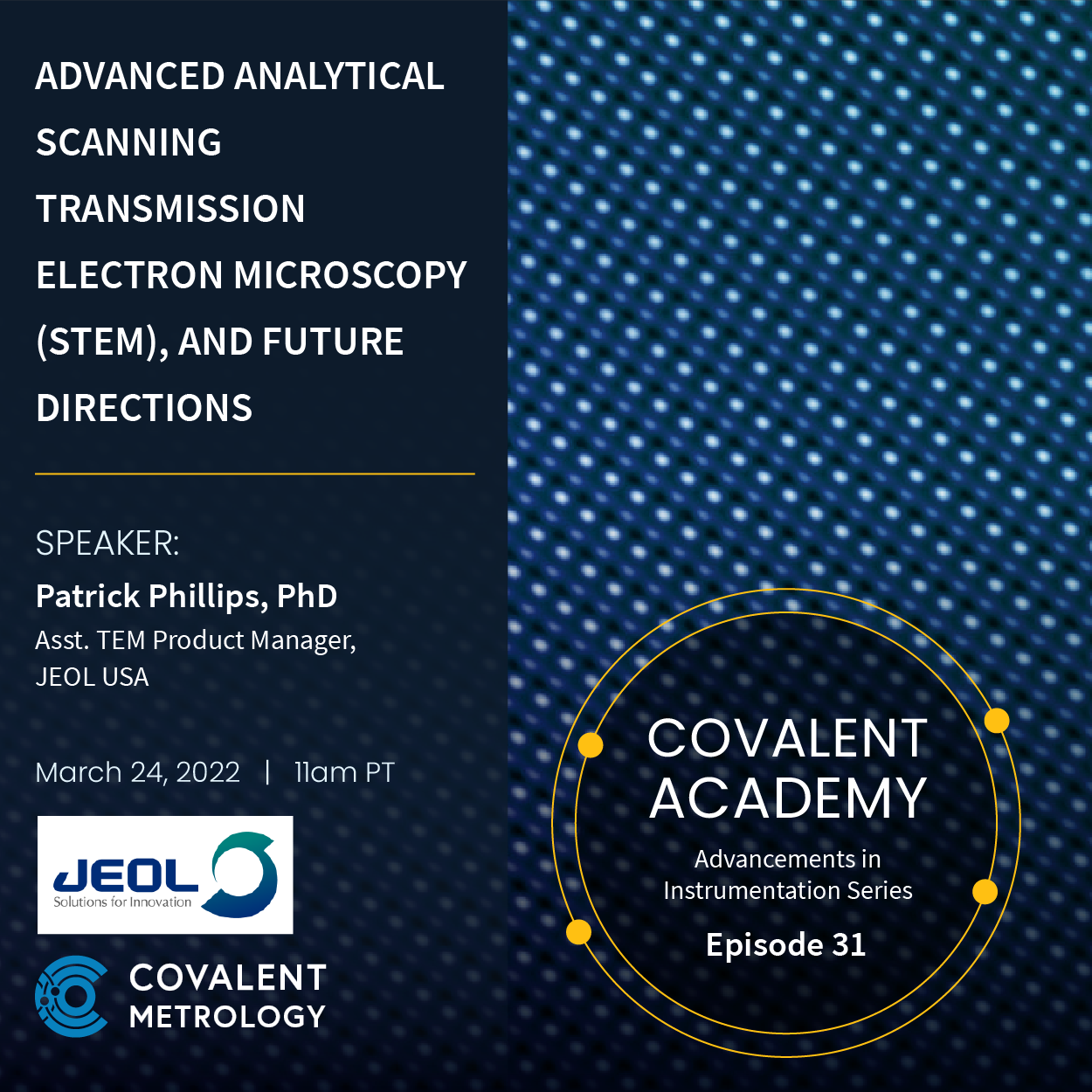
Advanced Analytical Scanning Transmission Electron Microscopy (STEM), and Future Directions
There has been increasing demand for so-called ‘workhorse’-type transmission electron microscopes as the technologies and techniques in (scanning) transmission electron microscopy (S/TEM) have evolved. Researchers and engineers from diverse industries depend on the unparalleled spatial resolution of S/TEM imaging for key structural insight into novel nanomaterials and devices, spurring recent developments of more flexible, reliable instrumentation.
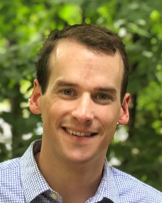
In this webinar, learn about the key features that have developed to facilitate accurate, atomic-scale S/TEM imaging for industrial applications. Guest speaker Dr. Patrick Phillips, Assistant TEM Product Manager at JEOL USA, will be exploring hardware and operational strategies to optimize image resolution, clarity, and insight from advanced S/TEM imaging techniques.
Attendees at the live webinar event will receive a bonus 10% discount off their next TEM project with Covalent (Terms and Conditions apply).
This Webinar Will Answer
- What advancements are incorporated in modern S/TEM instruments?
- What are the current capabilities of a conventional S/TEM outfitted with a cold field-emission gun?
- What new possibilities for analysis are possible with the current state-of-art S/TEM?
- How can non-aberration corrected S/TEM be used to investigate and optimize advanced materials and devices?
- How is the field of S/TEM expected to expand and advance in the coming years?
Aberration Correction Isn’t as Necessary as It Once Was
For decades, only aberration-corrected S/TEM instruments were able to achieve reliable atomic resolution; analysts came to infer that aberration-corrected microscopes – often costing upwards of a million dollars to purchase, let alone maintain – were practically a prerequisite for capturing images at atomic scale.
Today’s tools turn that preconception on its head. Enhancements to cold field-emission sources, large-area silicon drift detectors (SDDs) and increased stabilization in the electron optics of transmission electron microscopes help to ensure top-quality images even in the absence of aberration correction. Find out how these recent technologies coalesce with operational strategies to enable new kinds of analysis on advanced materials and devices.

About the Speakers

Patrick Phillips, PhD
Patrick received his PhD in Materials Science and Engineering in 2012 from the Ohio State University. Following an appointment as a Research Assistant Professor at the University of Illinois – Chicago, he joined JEOL USA in 2016. Previous research projects and current interests include Cs-Corrected STEM/EELS/EDS of metals, battery materials, oxides, and 2D structures.

About Covalent Metrology
Covalent Metrology is a disruptive analytical services laboratory and platform based in Sunnyvale, California. Its mission is to help companies who use advanced materials to get better data and insights more easily and affordably to facilitate faster development and production. Covalent is dramatically changing the characterization and imaging landscape by combining transparent pricing, data platforms, and top-notch customer service with world-class scientists, state-of-art tools, and strategic partnerships.
Covalent now has over 500 customers in 30+ industries.
Learn more at: https://staging-covalentmetrologyproduction.kinsta.cloud

