Attenuated Total Reflectance (ATR)
$99 Base price View My Quote RequestCathodoluminescence (CL)

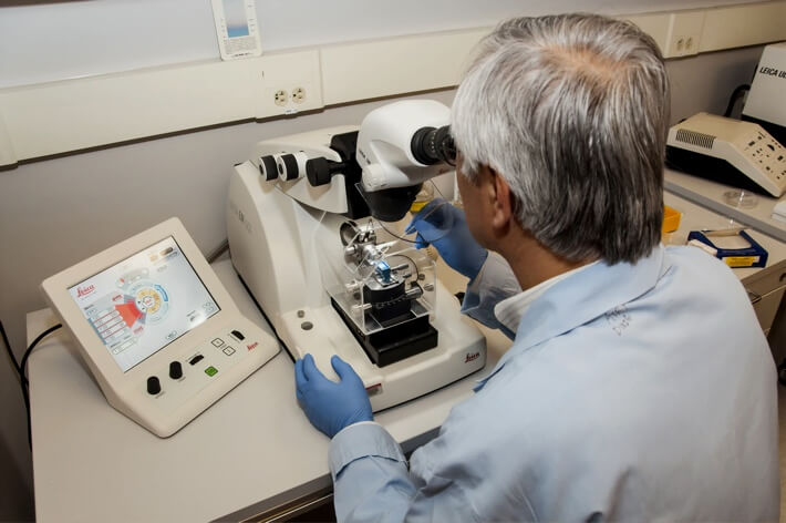
Cathodoluminescence (CL) is a combination microscopy and spectroscopy technique that produces high-speed spectral maps of optical emissions with nanoscale resolution. It is used to probe diverse features and properties of materials and devices, from the internal structures of direct bandgap semiconductors to surface plasmon resonances in metallic nanoparticles.
Strengths
- High speed spectral mapping
- High spatial resolution
- Wide wavelength range
- Suitable for in situ device analysis
- Specialized accessories accommodate cold experiments down to 30 K
Limitations
- Maximum area measured can be up to millimeter scale
- Sample will receive some damage by electron gun
- Organic materials are not ideal
Technical Specifications:
Learn More:
Instruments Used for CL
JEOL JSM-7100F/TTLS
- Wavelength Range: 200 – 1600 nm
- Acceleration Voltage: 0.5 – 30 kV
- Beam Current: up to 300 nA
- Measurement Area: 500 nm2 up to 1 mm2
- Temperature Range: Room Temp (~ 25 ⁰C)
- Cooling Unit can accommodate temperatures down to 30 K
- Cathodoluminescence Spectrometer is a Toray Original high-speed UV-Vis-NIR CL System based on HORIBA Jobin Yvon
- Detectors:
- CCD
- Photomultiplier (visible and near-infrared EM radiation)
- InGaAs multi-channel detector
How CL Works
The electrons from a scanning electron beam of an SEM are used to excite electrons across the energy gap of a semiconductor. When these electrons relax back to their resting state a photon can be emitted and cathodoluminescence (CL) measures the spectral energy and intensity of the emitted photons. In many ways it is like photo-luminescence except for that it uses an electron beam to excite the material as opposed to using a beam of light for the excitation source.
Using the electron beam in a scanning electron microscope as a non-destructive, broadband optical excitation source, cathodoluminescence analysis achieves the same nano-scale spatial resolution as scanning electron microscopy (SEM) techniques. A specialized detector mounted in the sample chamber measures the emitted photons, whose energies can be analyzed and mapped to probe fundamental and functional properties of the material.
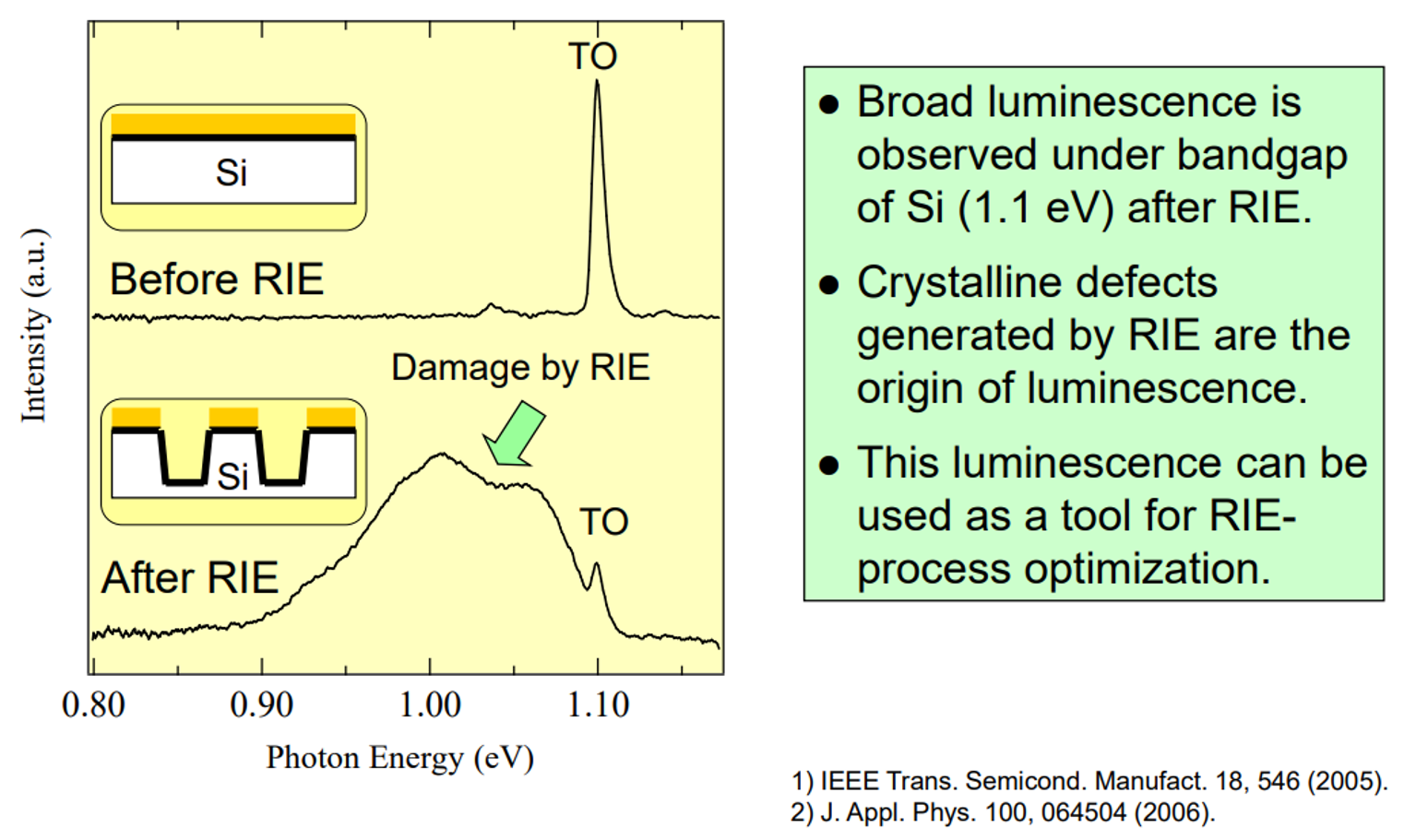
Cathodoluminescent photons are generated from a variety of coherent and incoherent processes. They can thus be used for both functional optical analysis and to study the electronic structure of solid-state materials. In particular, CL analysis is performed to investigate bandgaps and defects (which lower the CL intensity) in semiconductors, where it can be used to generate hyperspectral light emission maps that represent the local density of states. It is also seeing more recent use in metallic nanoparticle analysis, due to recent advances in detector technologies that facilitate greater collection efficiency from samples that intrinsically produce limited cathodoluminescence signal.
Additional Resources
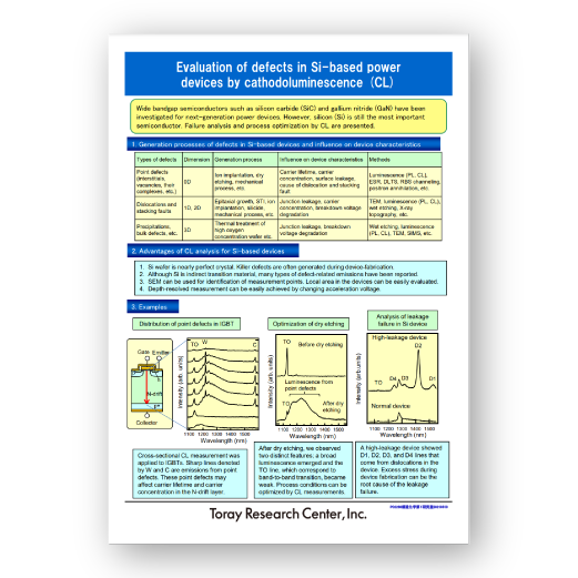
Evaluation of Defects in Si-based Power Devices by...
IN Publications
December 22, 2021
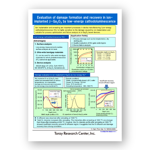
Evaluation of Damage Formation and Recovery in Ion...
IN Publications
December 22, 2021
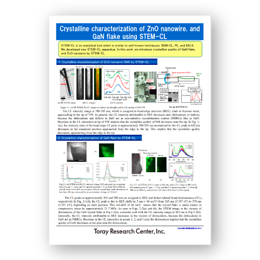
Crystalline Characterization of ZnO Nanowire and GaN Flake...
IN Publications
December 22, 2021
+
Add to Comparison
Focused Ion Beam Scanning Electron Microscopy (FIB-SEM)
In Microscopy & Imaging
FIB-SEM systems are used to produce 2D and 3D images of surface topography, and are able to resolve...
+
Add to Comparison
Scanning Electron Microscopy (SEM)
In Microscopy & Imaging
Scanning electron microscopy (SEM) is a surface imaging technique capable of achieving nm resolution on topographical features. Additionally,...
✕
Comparison link sent successfully
✕
Please use valid email address
✕
You need to have at least 2 techniques to compare
✕
You can select maximum 5 techniques
